 cognitora
Cognitora Edge AI
Bandwidth-first boards and clusters for local AI inference
Technical whitepaper, version 0.3, October 2026. EVT stage: the first carrier boards and the Edge Tower dock are designed, with schematics, layouts, BOMs priced from distributors and order files for JLCPCB and PCBWay (section 13). Production specifications are design targets. SoC, DRAM and RK1828 volume prices are estimates. Performance figures are marked as measured or estimated.
Abstract
Cognitora Edge AI is a family of small AI computers for robotics, home inference and low-energy clusters. The design rests on one observation: on small hardware, generating tokens from a language model is limited by memory bandwidth, not by compute. The family has three products.
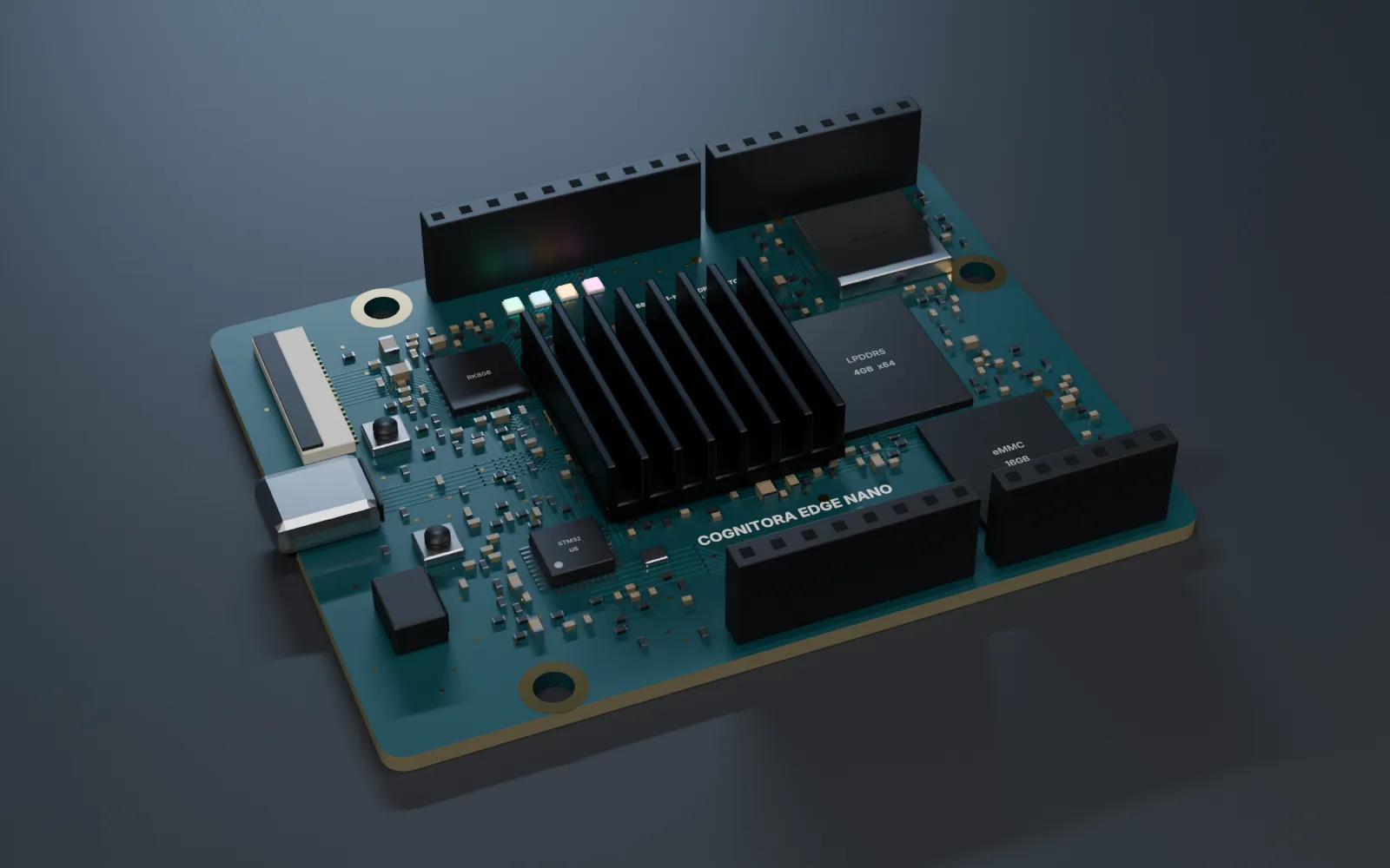
- Edge Nano, 68.85 x 53.34 mm, under $100 BOM. An RK3588S with a 64-bit LPDDR5 bus, a real-time MCU and 2.54 mm expansion headers, for robots and vision.
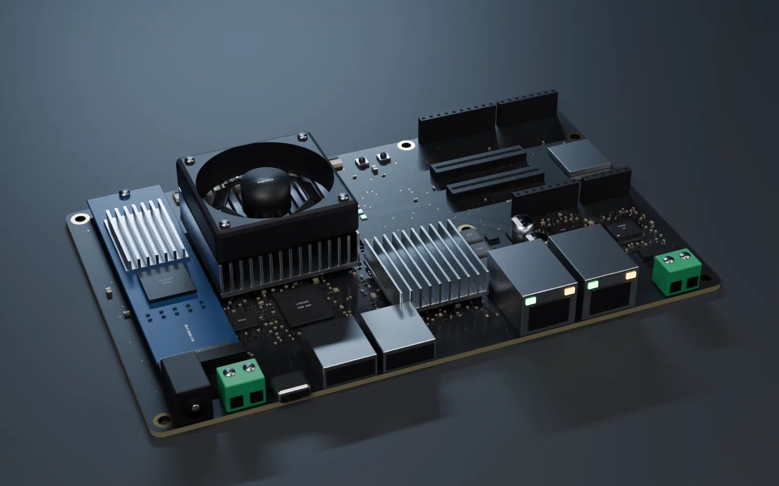
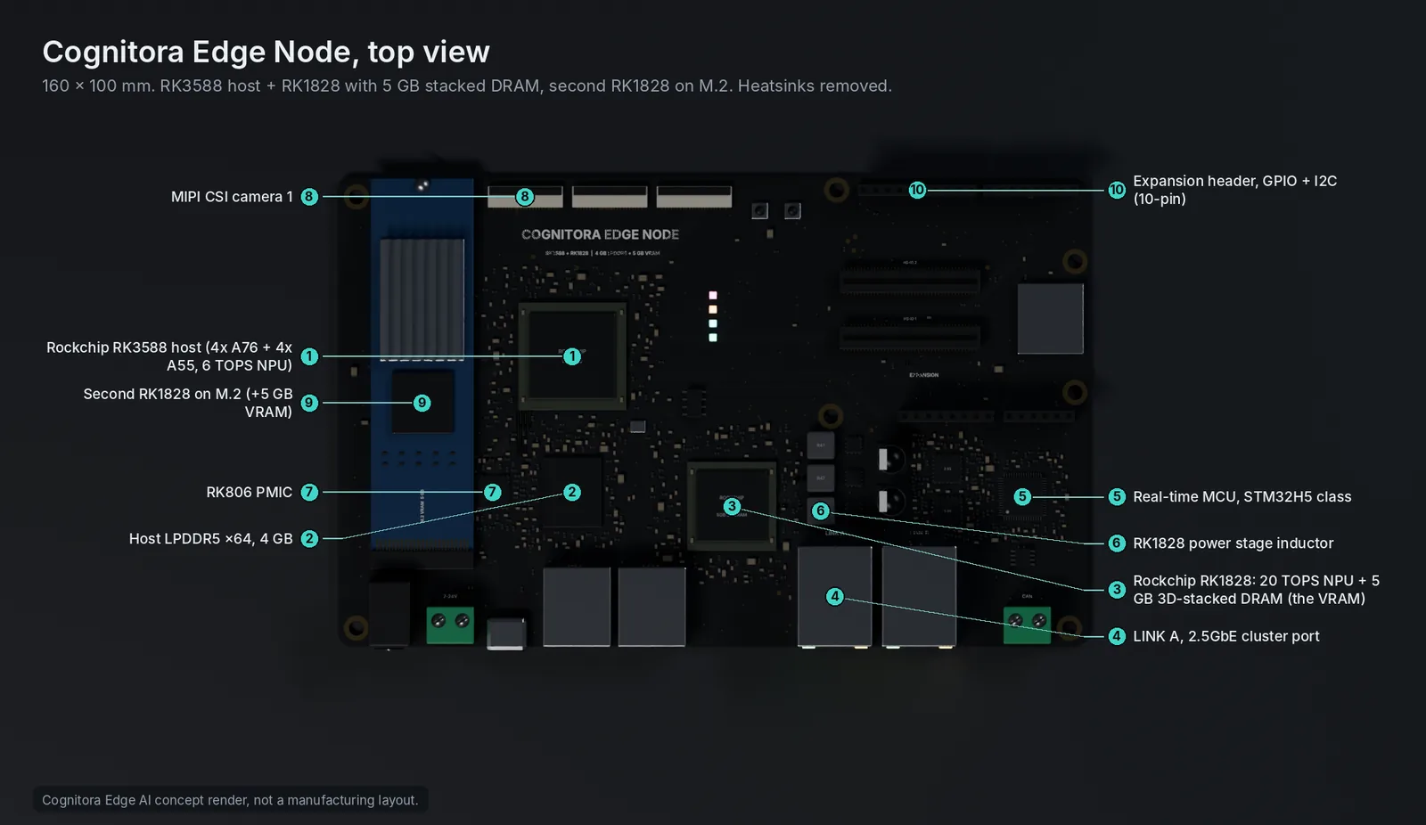
- Edge Node, 160 x 100 mm, about $305 BOM. An RK3588 host plus an on-board Rockchip RK1828 coprocessor whose 5 GB of 3D-stacked DRAM acts as VRAM. It decodes an 8B model at 61 tokens/s (measured on the RK1828).
- Edge Tower, four Edge Nodes standing in a dock board around one finned thermal core, cooled by one 160 mm fan. The dock links the nodes in a ring over their two 2.5GbE ports and leaves one 12 V input, one LAN port and two USB-C ports at the rear. With a second RK1828 per node it holds 40 GB of VRAM and runs a 32B model at about 13 tokens/s (estimate).
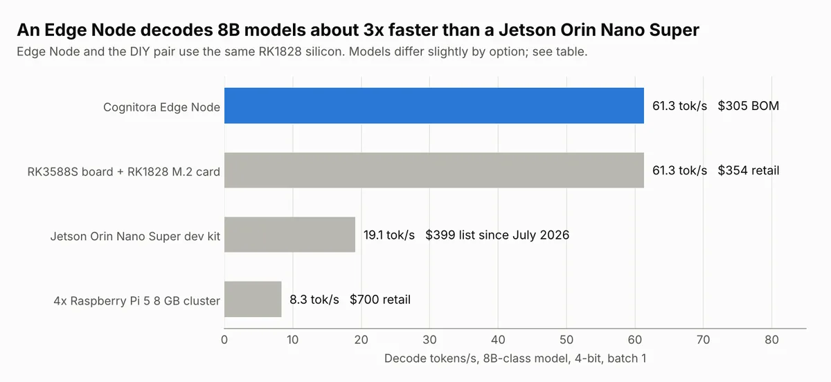
On 8B-class models an Edge Node decodes about 3x faster than a Jetson Orin Nano Super and about 7x faster than a four-board Raspberry Pi 5 cluster, at a lower BOM than either one's retail price.
1. The problem: decode is a bandwidth equation
A language model generates one token at a time. For each token at batch size 1, the accelerator reads every weight once, plus the KV cache built so far. The arithmetic per byte is tiny: about 2 operations per weight. Speed therefore follows memory bandwidth:
tokens/s ~ effective_bandwidth / (weight_bytes + kv_bytes_per_token x context)
Measured results on the RK3588 fit this closely. llama.cpp on four Cortex-A76 cores runs Qwen2.5-1.5B (Q4_K_M, about 1 GB of weights) at 22.57 tokens/s and Qwen2.5-7B (about 4.7 GB) at 5.44 tokens/s [1]. Both imply 22 to 25 GB/s of effective bandwidth. Adding TOPS does not move these numbers. Adding bandwidth does.
Memory is now the budget
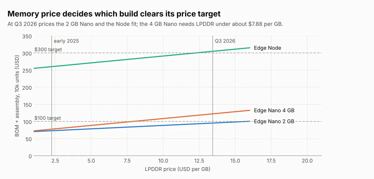
DRAM prices rose sharply through 2026. A 12 GB LPDDR5X chip cost $77.1 in Q1 2026 and $145.9 in Q2 2026, about $12.2 per GB at the largest buyers' contract prices [2]. TrendForce expects mobile DRAM to rise another 8 to 13% in Q3 2026 and to hold at that level through Q4 [3]. Raspberry Pi reports LPDDR4 up sevenfold in a year [4]. This model uses about $13.4 per GB for Q3 2026.
Three consequences shape the design:
- Capacity picks the model, bandwidth picks the speed. Every GB costs about $13, so a sub-$100 board carries 2 to 4 GB and targets 1.7B to 4B models.
- A second memory pool only pays when it adds bandwidth. A separate VRAM chip at host-like bandwidth buys the same bytes twice. The RK1828's stacked DRAM earns its place because it is about 10x faster than the host LPDDR.
- Bus width comes in packages. A 128-bit bus means two x64 packages and 8 GB or more. One x64 package is the widest bus a $100 board can afford.
2. Design principles
| Principle | Mechanism | Where |
|---|---|---|
| Bandwidth per TOPS is the headline metric | One x64 LPDDR5 package per host, stacked DRAM beside the accelerator | All boards |
| One coherent memory domain | Coherent NoC, SMMU with shared virtual memory, zero copy | Gen B |
| Partition, do not time-slice | Arm MPAM cache and bandwidth partitions, pinned big cores for the agent loop | Gen B, cpusets on Gen A |
| Software-managed on-chip SRAM | 4 MB system cache with residency control | Gen B |
| Low precision with 2:4 sparsity | Tensor engine with INT4/INT8 and 2:4 support | Gen B |
| Decode weights in the memory path | Weight-decode DMA for 4-bit block formats | Gen B |
| Hard partitions between workloads | NPU cores or slices per workload with bandwidth floors | All boards |
| Prebuilt command graphs | One command list per decode step | Runtime |
| Fast memory next to the accelerator | RK1828 with 5 GB stacked DRAM | Edge Node |
| Scale out without a switch | LINK A/B 2.5GbE chain or ring, pipeline parallel | Edge Node, Edge Tower |
| Shared cooling | One finned core and one 160 mm fan for four nodes | Edge Tower |
3. Product family
| Edge Nano | Edge Node | Edge Tower | |
|---|---|---|---|
| Size | 68.85 x 53.34 mm | 160 x 100 mm | 182 mm diameter, 264 mm tall |
| Host | RK3588S: 4x Cortex-A76 + 4x Cortex-A55, Mali-G610, 6 TOPS NPU | RK3588, same cores, more PCIe | 4x Edge Node |
| Host memory | 2 or 4 GB LPDDR5, x64 | 4 GB LPDDR5, x64 | 16 GB total |
| VRAM | None (protected zone of host LPDDR) | RK1828: 20 TOPS INT8, 5 GB stacked DRAM, plus M.2 slot for a second RK1828 | 20 GB, or 40 GB with M.2 cards |
| Real-time MCU | STM32U5 class, Zephyr RTOS | STM32H5 class + CAN-FD | 4x |
| Networking | Wi-Fi 5, Bluetooth | 2x 2.5GbE (LINK A, LINK B) + management port | LINK ring on the dock, 5-port switch for the management ports, one rear LAN port |
| I/O | USB-C, expansion headers, Qwiic, MIPI CSI | USB-C, 2x USB 3, 3x MIPI CSI, expansion headers, 2x high-speed I/O, microSD, dock card edge | Rear: RJ45, USB-C (service, all nodes), USB-C (host, head node) |
| Power | USB-C, 5 V at 3 A | 12 to 24 V jack, 7 to 24 V terminal, 12 V from the dock | One 12 V input (XT60), 300 W class supply |
| BOM, 10k units, Q3 2026 DRAM | About $95 (2 GB), $122 (4 GB) | About $305 | About $1,290 (4 nodes and the dock), plus $249 per M.2 card at retail |
| Decode | Qwen3-1.7B about 23 tok/s (est.) | Qwen3-8B 61 tok/s (measured) | Qwen3-32B about 13 tok/s (est.) |
4. Architecture
Two silicon generations share one architecture.
4.1 Gen A: shipping silicon
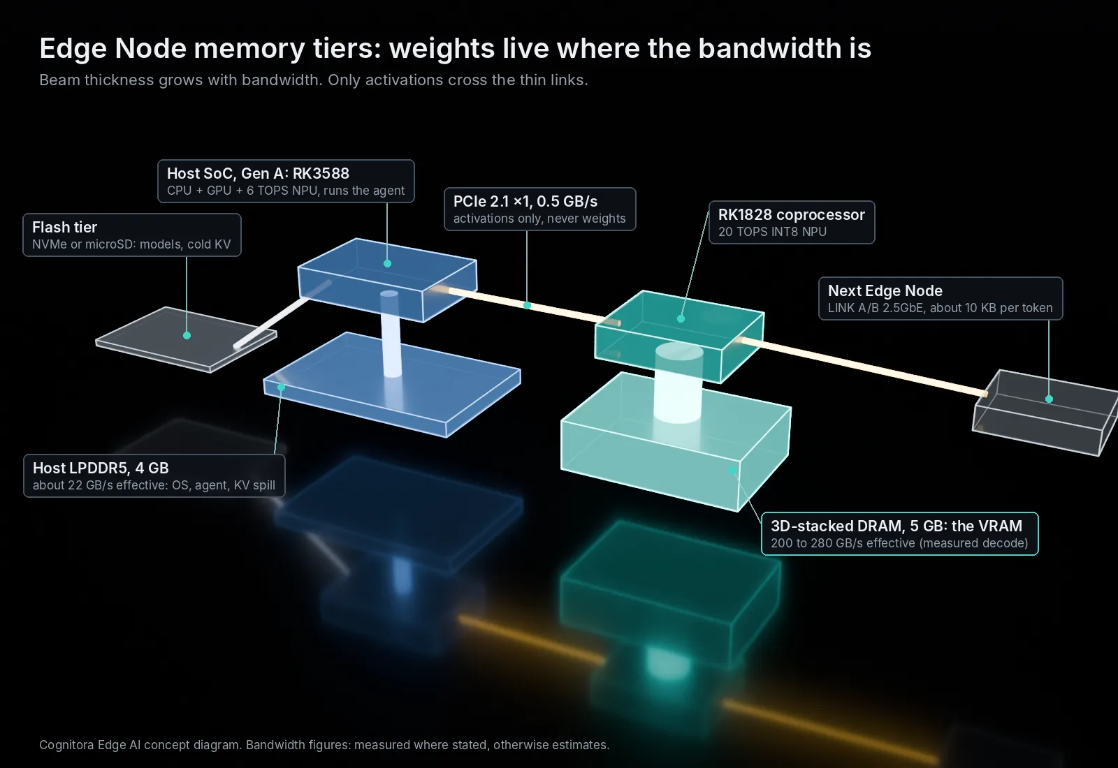
Gen A uses Rockchip RK3588 and RK3588S. The CPU runs the agent: tokenizer, sampler, tool calls and sandboxes. The Mali GPU handles display and pre and post-processing. The 6 TOPS NPU in three cores runs vision and small language models. On the Edge Node the RK1828 runs the language model from its own stacked DRAM and talks to the host over PCIe 2.1 x1. Memory sharing on the host uses dma-buf buffers with zero copy.
4.2 Gen B: target SoC specification
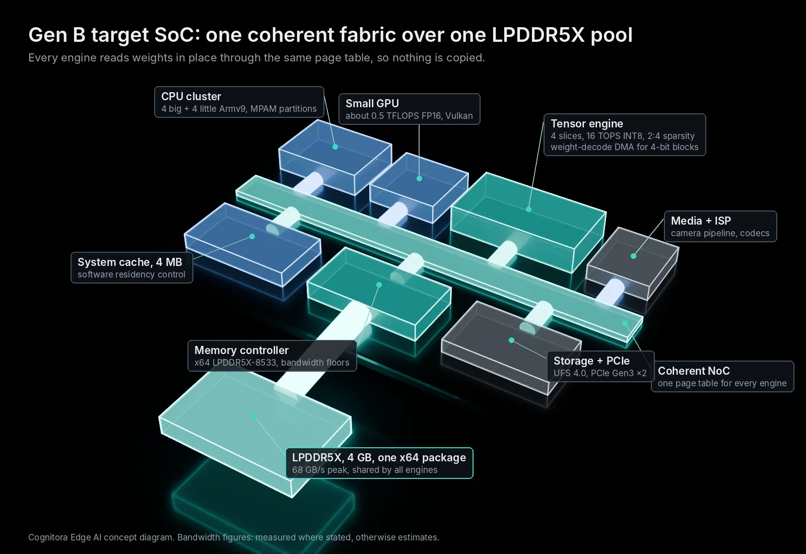
Gen B is the SoC the family wants next. It is written as a requirements specification for a vendor SoC (the RK3668 class, announced with LPDDR5/5X/6 up to 100 GB/s and a 16 TOPS NPU [5]) or for licensed IP, not as a from-scratch tapeout.
| Block | Specification |
|---|---|
| CPU | 4 big + 4 little Armv9 cores, Arm MPAM cache and bandwidth partitions |
| GPU | About 0.5 TFLOPS FP16, Vulkan compute |
| Tensor engine | 4 slices, 16 TOPS INT8 dense, INT4, 2:4 structured sparsity, 512 KB SRAM per slice |
| Weight-decode DMA | Expands GGUF-style 4-bit blocks and 2:4 metadata in flight, so DRAM moves about 4.5 bits per weight |
| System cache | 4 MB with software residency control |
| Memory | One x64 LPDDR5X-8533 package, 68 GB/s peak, about 48 GB/s effective, 4 GB |
| Fabric | Coherent NoC, SMMU with shared virtual addressing: every engine walks the same page tables |
| Storage and I/O | UFS 4.0, PCIe Gen3 x2 |
5. Memory hierarchy
| Tier | Edge Nano (Gen A) | Edge Node (Gen A) | Gen B target | What lives there |
|---|---|---|---|---|
| T0 on-chip SRAM | NPU buffers, 3 MB L3 | NPU buffers, 3 MB L3 | 4 MB system cache + 4 x 512 KB scratchpad | Activations, hot KV window, dequant scales |
| T1 host LPDDR | 2 or 4 GB LPDDR5, about 22 GB/s effective | 4 GB LPDDR5 | 4 GB LPDDR5X-8533, 68 GB/s peak | OS, agent sandboxes, small models, KV spill |
| T1b stacked-DRAM VRAM | None | RK1828, 5 GB, 200 to 280 GB/s effective (from measured decode) | Same as Edge Node | Weights and KV for models up to 8B per RK1828 |
| T2 flash | eMMC 16 GB or microSD | NVMe on M.2 or microSD | UFS 4.0 or NVMe | Model store, LoRA adapters, idle-session KV |
Zones in host memory. A V-zone holds weights and KV cache: a physically contiguous carve-out from a dma-buf heap, mapped with 2 MB pages. An S-zone holds the OS and agent sandboxes, capped per sandbox with cgroups v2 so a runaway tool cannot evict the model.
Memory budget, Edge Nano. Values in GB, 4-bit weights, INT8 KV at 4k context.
| Use | 2 GB build | 4 GB build |
|---|---|---|
| OS, drivers, agent runtime | 0.50 | 0.60 |
| Model weights | Qwen3-1.7B: 0.97 | Qwen3-4B: 2.26 |
| KV cache, 4k tokens, INT8 | 0.23 | 0.30 |
| Vision model and camera buffers | 0.10 | 0.15 |
| Headroom | 0.20 | 0.69 |
6. The VRAM tier: RK1828
The RK1828 is a Rockchip AI coprocessor with a 20 TOPS INT8 NPU and 5 GB of 3D-stacked DRAM inside the package, claimed at 1 TB/s. It supports INT4, INT8, INT16, FP8, FP16 and BF16, and connects to the host over PCIe 2.1 x1 [6].
Measured decode, Rockchip RKNN3 runtime, 128 input and 128 output tokens, W4A16 [7]:
| Model | Decode tok/s | Time to first token | Implied effective bandwidth |
|---|---|---|---|
| Qwen3-1.7B | 139.4 | 54 ms | 135 GB/s |
| Qwen3-4B | 88.5 | 110 ms | 200 GB/s |
| Qwen3-8B | 61.3 | 182 ms | 283 GB/s |
Implied bandwidth rises with model size because fixed per-token overheads matter less. The model uses 250 GB/s for larger shards. Under a 7B load the module averages 13.6 W and peaks at 29.4 W [6], so the Edge Node power stage is sized for 30 W and the host power-gates the RK1828 at idle.
The PCIe 2.1 x1 link (0.5 GB/s) sets one hard rule: weights never cross it at run time. Each model slice stays resident in stacked DRAM. Only activations and token IDs cross.
7. Board-to-board link and clusters
Each Edge Node has two 2.5GbE ports, LINK A and LINK B. Standalone nodes chain A to B with short patch cables, no switch, and the head node bridges the chain to the home network.
In the Edge Tower there are no cables between nodes. Each node stands in a slot on a dock board in the base and brings its Ethernet out on its card edge, on the cable side of its own magnetics, so the same port works on the RJ45 or on the dock. The dock connects LINK B of each node to LINK A of the next as PCB traces, which closes a four-node ring. The nodes' management ports go to a 5-port gigabit switch on the dock (Microchip KSZ9567) whose fifth port is the tower's one LAN jack. The dock also carries 12 V to every slot, a USB hub that gives one rear USB-C port access to every node's console and flashing port, a second USB-C port for the head node, the CAN bus and the fan.
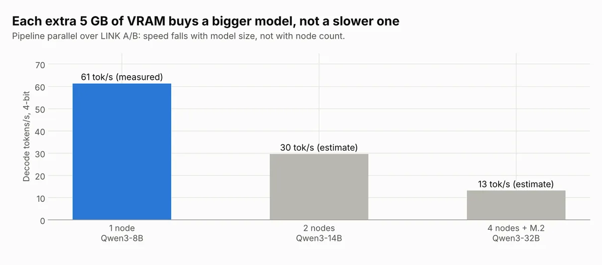
Pipeline parallelism. The model is split by layers. Node 1 holds the first quarter of the layers, node 4 the last. For each token, only the hidden state crosses a boundary: 2 bytes x hidden size, about 10 KB for a 32B model. At 2.5 Gbit/s that is about 33 microseconds on the wire.
Latency budget per hop (estimate). RK1828 to host over PCIe, host to host over 2.5GbE, host to RK1828: about 0.25 ms. A 32B model on 8 RK1828s streams 18.4 GB of weights per token at 250 GB/s, about 74 ms. Eight hops add about 2 ms, under 3%.
| Model | Nodes | RK1828 cards | VRAM | 4-bit weights | Max INT8 KV context | Decode | Basis |
|---|---|---|---|---|---|---|---|
| Qwen3-8B | 1 | 1 | 5 GB | 4.6 GB | 3k | 61.3 tok/s | Measured |
| Qwen3-14B | 2 | 2 | 10 GB | 8.3 GB | 16k | 29.6 tok/s | Estimate |
| Qwen3-32B | 4 | 8 (with M.2) | 40 GB | 18.4 GB | 40k (model limit) | 13.2 tok/s | Estimate |
Pipeline parallelism scales capacity, not single-stream speed: one token still visits every stage in turn. With several users, each stage works on a different request, so aggregate throughput grows with node count.
8. Edge Tower thermal design
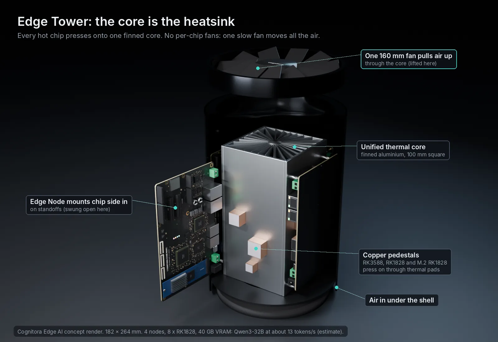
The Edge Tower turns four boards into one cooling system. Instead of a heatsink and a small fan on every chip, every hot chip presses onto one shared, finned core, and one slow fan moves all the air.
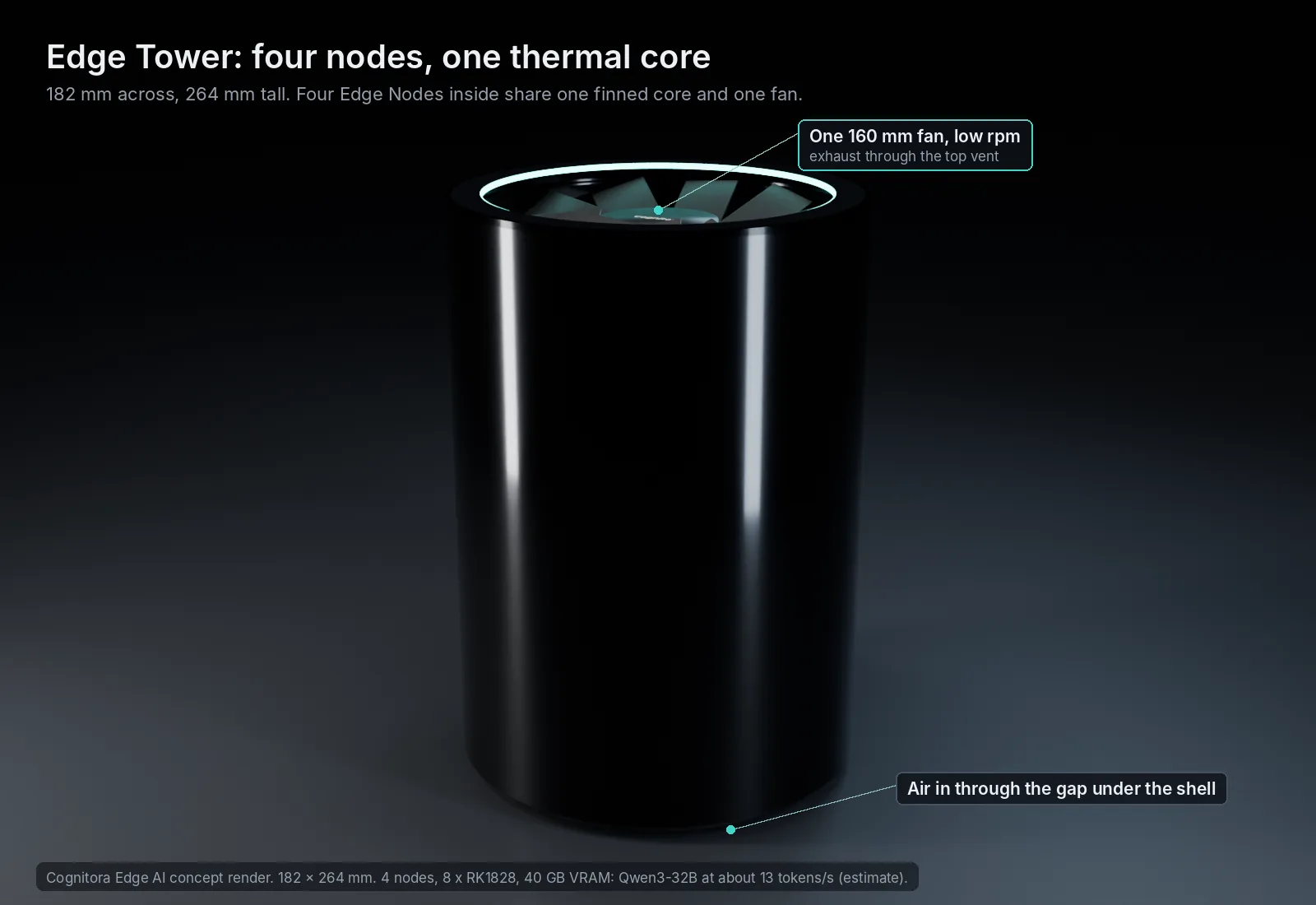
- Unified thermal core. A 100 mm square aluminium extrusion runs up the middle of the tower, with 28 radial fins inside.
- Boards chip side in. Each Edge Node stands in a vertical slot on the dock, 16 mm from one face of the core, components facing the core. The tallest part (RJ45, 13.5 mm) clears the core face.
- Dock in the base. A round 4-layer board under the core holds the four slots and all inter-node wiring. A 92 mm opening in its centre lets the intake air reach the core. Its rear tongue carries the only external connectors: 12 V (XT60), LAN (RJ45) and two USB-C.
- Copper pedestals. The RK3588, the on-board RK1828 and the M.2 RK1828 press onto copper pedestals machined on the core face, through 0.5 mm thermal pads. No per-chip heatsinks, no per-chip fans.
- One slow fan. A 160 mm fan in the top of the shell pulls air in through an 8 mm gap under the shell, through the dock's opening and up through the core fins.
- Fan-stop at idle (design target). At idle each node power-gates its RK1828s, the tower drops to about 15 W (estimate), and the core works as a convection chimney.
| Heat source per node | Average | Peak |
|---|---|---|
| RK1828, on board | 13.6 W | 29.4 W |
| RK1828, M.2 card | 13.6 W | 29.4 W |
| RK3588 host | about 5 W | about 8 W |
| Carrier (NICs, regulators) | about 3 W | about 4 W |
| Per node | about 35 W | about 71 W |
| Tower, four nodes | about 140 W | about 284 W |
RK1828 figures are measured [6]; host and carrier figures are estimates. The enclosure is 182 mm across and 264 mm tall. The thermal design is a target: a four-node prototype with thermocouples on every pedestal is on the roadmap.
9. Software stack
- OS layer. Linux with dma-buf heaps for the V-zone, cgroups v2 and cpusets for the S-zone, resctrl-style MPAM controls on Gen B.
- One model format. GGUF on disk. Gen A runs llama.cpp on the CPU and Mali GPU (Vulkan) and RKLLM on the NPU. The RK1828 runs RKNN3 models. Gen B adds a GGML backend whose weight-decode DMA reads GGUF blocks directly.
- Accelerator partitions. On the RK3588 NPU, one core for always-on vision and two for the LLM.
- Prebuilt decode step. One recorded command list per decode step, replayed every token.
- KV manager. Paged INT8 KV cache, a shared prefix cache for system prompts and tool schemas, spill of idle sessions to flash.
- Speculative decoding. A small draft model proposes several tokens and the main model verifies them in one weight pass. The gain depends on acceptance rate and must be measured per workload.
- Agent runtime on the big cores. Tokenizer, grammar-constrained sampling for tool calls, and WebAssembly sandboxes pinned to the Cortex-A76 cluster.
- Pipeline runtime. A stage daemon per node, stage assignment by layer count and free VRAM, activations over LINK A/B.
- Real-time MCU. Motor, IMU and CAN-FD loops on Zephyr, bridged to Linux over RPC. The MCU also wakes the host on voice, network or sensor events.
- Bandwidth telemetry. DDR performance counters feed admission control.
10. Performance summary
Single board, 4-bit weights, short context:
| Model | Edge Nano (est.) | Gen B target (est.) | Edge Node (measured) |
|---|---|---|---|
| Qwen3-1.7B | 22.7 tok/s | 49.4 tok/s | 139.4 tok/s |
| Qwen3-4B | 9.7 tok/s (4 GB build) | 21.1 tok/s | 88.5 tok/s |
| Qwen3-8B | Does not fit | Does not fit | 61.3 tok/s |
Energy. An Edge Node under an 8B load draws about 18.6 W (13.6 W RK1828 average [6] plus about 5 W for the host, estimate), about 3.3 tokens per joule. A Jetson Orin Nano Super at its 25 W mode delivers 19.1 tok/s on Llama 3.1 8B [8], about 0.8 tokens per joule at that power.
11. Cost
BOM plus assembly at 10k units, LPDDR at about $13.4 per GB (Q3 2026). Volume SoC and RK1828 prices are estimates. The carrier lines (board controller, connectors, passives and ESD, the 12 V input stage) use the EVT BOM's distributor prices at qty 1000 (section 13), which added $24 to the Edge Node and $3.50 to the Edge Nano over the concept estimates. The Edge Tower is four Edge Nodes plus the dock, whose lines also come from its EVT BOM at qty 1000 (about $68 built); the thermal core, shell, fan and power supply are not included. Full line items are in docs/data/bom_edge_nano.csv, docs/data/bom_edge_node.csv and docs/data/bom_edge_tower_dock.csv.
| Configuration | BOM at Q3 2026 DRAM | BOM at early-2025 DRAM |
|---|---|---|
| Edge Nano, 2 GB | $95 | $73 |
| Edge Nano, 4 GB | $122 | $78 |
| Edge Node | $305 | $260 |
| Edge Tower, 4 nodes and the dock | $1,287 | $1,108 |
The 4 GB Edge Nano falls under $100 once LPDDR drops below about $7.88 per GB, between the Q1 2026 level (about $6.4 per GB) and the Q2 2026 level. The same PCB takes both memory sizes.
12. Alternatives
8B-class dense models, 4-bit, batch 1. Cognitora figures are BOM, the others are list or retail prices, so prices are not like for like. At a 1.4x retail markup an Edge Node would sell for about $427, close to the $399 of a Jetson Orin Nano Super, with about 3x its decode speed.
| Option | Price | Decode | Model | tok/s per $100 | Source |
|---|---|---|---|---|---|
| Cognitora Edge Node | $305 BOM | 61.3 tok/s | Qwen3-8B | 20.1 | RK1828 measured [7] |
| RK3588S board + RK1828 M.2 card | about $354 retail | 61.3 tok/s | Qwen3-8B | 17.3 | Same silicon [6][9] |
| Jetson Orin Nano Super dev kit | $399 list since July 2026 | 19.1 tok/s | Llama 3.1 8B | 4.8 | [8][10] |
| 4x Raspberry Pi 5 8 GB cluster | about $700 retail | 8.3 tok/s | DeepSeek-R1-Distill-Llama-8B, Q40 | 1.2 | [4][11] |
A Raspberry Pi 5 with the AI HAT+ 2 (Hailo-10H, 8 GB, $130 for the HAT) reaches up to about 8 tok/s on 1 to 1.5B models and does not run 8B models [12].
13. From concept to EVT hardware
The first hardware is an engineering-validation (EVT) build of each board as a carrier for a bought-in compute module. The module brings the SoC, DRAM and accelerator that already work, so the first spin tests what the carrier adds: power, I/O, the board controller, the RK1828 power path, the tower mechanics and thermals. The carrier circuits carry over to the chip-down production boards.
| Edge Node EVT | Edge Nano EVT | |
|---|---|---|
| Board | 160 x 100 mm, 6 layers, single-sided assembly | 68.85 x 53.34 mm, 4 layers, two-sided assembly |
| Host module | 260-pin SO-DIMM (Jetson Orin NX/Nano pinout): Turing RK1 with RK3588 | CM4-format connector: Radxa CM5 with RK3588S2 |
| VRAM | 2x M.2 2280 for DFRobot DFR1263 (RK1828) cards, switched 12 V per card | |
| Board controller | STM32G474: power sequencing, card power, fan, 4 NTCs, CAN-FD | STM32L552: expansion headers, Qwiic |
| Links and I/O | MGMT + LINK A/B (2x RTL8111H, 1GbE for EVT), 2x USB 3, USB-C, 2x MIPI CSI-2 | USB-C (power and USB 2.0), MIPI CSI-2 x4 |
| Parts | 313 footprints, 82 BOM lines | 60 footprints, 34 BOM lines |
The KiCad projects are generated by Python in hardware/evt/gen/, so every pin assignment can be reviewed as code.
Pinouts and sub-circuits come from machine-readable open designs: Antmicro's Jetson Orin baseboard
(Apache-2.0) supplies the SO-DIMM pin functions and the bucks, eFuses, M.2 slot, USB power switches
and ESD, copied with their parts and values. Both schematics pass KiCad's ERC with no errors or
warnings, and the exported netlist is checked back against the intended connections. Placement is
DRC-clean on both boards. Routing is a Freerouting first pass.
Cost of the EVT build. From the real BOM, distributor prices taken on 8 October 2026, and JLCPCB's assembly price rules:
| Edge Node | Edge Nano | |
|---|---|---|
| Carrier parts, 10-board build | $81 | $24 |
| Carrier built (parts, assembly, bare board) | $117 | $42 |
| Modules | RK1 $379 + 2x DFR1263 $498 | Radxa CM5 4/32 GB $80 |
| EVT unit | about $994 | about $122 |
At qty 1000 the carrier parts come to $57 (Node) and $17 (Nano). Line by line against the concept estimates, connectors and passives were underestimated (Node connectors $19 against $8, passives and ESD $10 against $4) and Ethernet was overestimated. Section 11 now uses the EVT figures.
What the EVT pass changed. - The reference design's RJ45 jack is superseded, so the Node uses jacks from the KiCad library. - The RK1828 AUX outputs got a 3 A circuit breaker. The reference value would have allowed 6 A into a card cable. - The host kill switch got a gate pull-down, so the host stays on while the controller is in reset. - The expansion headers moved onto the standard 68.6 x 53.3 mm pattern. - Mounting holes now keep standoff screws clear of bottom-side parts.
Not yet ready to order. The PCIe, USB 3, CSI-2 and Ethernet pairs are autorouted without length
matching or impedance-checked geometry. They need a hand-routing pass and a signal-integrity sign-off
before Gerbers go out. At bring-up, the RK1's PCIe and USB 3 lane mapping is checked against its
device tree. Details and the full bring-up list are in hardware/evt/README.md.
14. Risks and roadmap
| Risk | Impact | Mitigation |
|---|---|---|
| LPDDR stays near $13 per GB through 2027 | 4 GB Edge Nano stays above $100 | Ship the 2 GB build as the $100 SKU |
| RK1828 volume price unknown (estimate $100 to $150) | Edge Node BOM moves by up to $30 | Vendor quote before layout; M.2 card as fallback |
| RK1828 multi-card pipelining | Cluster numbers depend on the vendor toolkit | Validate on two nodes before the tower |
| PCIe 2.1 x1 between host and RK1828 | Weights cannot stream from host memory | Keep each model slice resident in stacked DRAM |
| 4-bit quality on small models | Weaker tool calling | Benchmark tool-call accuracy; keep embeddings and head at 8 bits |
| Edge Tower thermals | Fan-stop idle mode unproven | Thermal test on a four-node prototype |
| Gen B silicon | A specification, not a product | Track RK3668-class parts |
| Edge Node BOM above $300 | $305 with qty-1000 carrier prices | Cost-down at DVT: one AUX terminal, an STM32G4 part with less flash in the same package, 10k pricing |
| Board controller supply | STM32G474 at a 52-week lead time at the check | Buy EVT stock early; qualify a second STM32G4 part |
| Autorouted high-speed nets | EVT boards not yet SI-clean | Hand-route PCIe, USB 3, CSI-2 and MDI with length tuning before release |
Roadmap
- Validate on existing hardware: an RK3588S board plus an RK1828 M.2 card. Gate: Qwen3-8B at 55 tok/s or more, two-card pipelining works.
- EVT carriers for bought-in modules (this revision, section 13), then chip-down Edge Nano and Edge Node layouts. Gate: carriers bring up, BOM quotes at or under $100 and $300.
- Runtime: V-zone daemon, NPU partitioning, KV manager, speculative decoding, pipeline over LINK A/B.
- Edge Tower prototype. Gate: no thermal throttling at full load.
- Gen B: evaluate RK3668-class samples. Gate: 45 GB/s or more effective and a landed SoC price at or under $30.
15. Reproduce
python3 model/perfmodel.py                 # tables, docs/data/*.csv, docs/figures/*.png
python3 hardware/specs.py                  # board JSON specs
pip install bpy==5.2.2                      # Blender as a Python module
python3 render/blender/render_boards.py     # board renders
python3 render/blender/render_cluster.py    # Edge Tower
python3 render/blender/render_diagrams.py   # 3D architecture diagrams
python3 web/viewer/build_viewer.py          # interactive viewer, web/viewer/index.html
References
- Turing Pi, "LLM inference benchmarks on RK3588: GGUF quantization", https://turingpi.com/llm-inference-benchmarks-rk3588-gguf-quantization/
- Wccftech, citing Sigmaintell, LPDDR5X 12 GB chip cost Q1 and Q2 2026 (June 23, 2026), https://wccftech.com/apple-is-in-for-a-sticker-shock-in-q3-with-lpddr5x-dram-costs-surging-by-68-8-in-a-single-quarter-as-operating-profit-margin-for-general-purpose-dram-to-hit-90-within-the-year/amp/
- TrendForce, Mobile DRAM contract price 3Q26, https://www.trendforce.com/research/download/RP260803NC
- BGR, "Not even the Raspberry Pi is safe from the RAM crisis" (April 23, 2026), https://www.bgr.com/2150106/raspberry-pi-cost-ram-crisis/
- CNX Software, Rockchip RK3668 and RK182X announcement (July 2025), https://cnx-software.com/2025/07/18/rockchip-unveils-rk3668-10-core-arm-cortex-a730-cortex-a530-soc-with-16-tops-npu-rk182x-llm-vlm-co-processor
- DFRobot, RK1828 AI accelerator M.2 module (DFR1263), https://www.dfrobot.com/product-3142.html
- DFRobot wiki, RKNN3 supported models and performance, https://wiki.dfrobot.com/dfr1263/docs/24735
- NVIDIA Technical Blog, Jetson Orin Nano Super, https://developer.nvidia.com/blog/?p=93942
- Orange Pi 5 Pro 4 GB LPDDR5 price history, https://pricehistory.app/p/orange-pi-5-pro-4gb-lpddr5-rk3588s-zur6eOyp
- Notebookcheck, "Nvidia quietly increases Jetson prices by up to 101%" (July 22, 2026), https://www.notebookcheck.net/Nvidia-quietly-increases-Jetson-prices-by-up-to-101.1348323.0.html
- Zenodo, DeepSeek-R1-8B on four Raspberry Pi 5, https://zenodo.org/records/20411979
- Hardware Corner, "Local LLMs on Raspberry Pi: what the AI HAT+ 2 can and cannot do", https://www.hardware-corner.net/local-llms-raspberry-pi-ai-hat-plus-2/
- Qwen3 model configurations, https://huggingface.co/Qwen